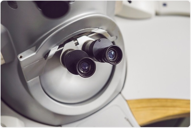
Electron microscopes are tools of paramount importance for scientists in the field of life science and material science. (TEM) is a microscopy technique that uses electrons instead of light to produce detailed images of the structure of elements.

Credit: Elizaveta Galitckaia/ Shutterstock.com
They have the capability of imaging defects ranging from those in a single column of atoms, to crystals, to even those at the scale of a nanometer.
The principle of a TEM is the use of electrons of very short wavelengths that enable a significantly higher resolution of images to be achieved than with the light microscope. TEMs have found tremendous applications, especially in research related to cancer, virology, nanotechnology, and semiconductors.
Need for extending TEM capabilities
Some drawbacks of TEM are the (a) need to prepare samples that are adequately thin and transparent for electrons; (b) altered biological samples due to exposure to electron beams; and (c) because of the small field-of-view the analyzed portion of sample may not be a true representation of the entire sample.
For such reasons, developments are ongoing for extending TEM. The resolution information acquired in electron microscopy is based on the specimen properties, preparation method, features of the TEM method, and imaging specifics. Modifications in these four aspects are considered when extending the capabilities of TEM. A few extensions of TEM are as follows;
Scanning TEM
The scanning TEM (STEM) is an improved mode of the conventional scanning electron microscope. Here, the microscope lenses are arranged in such a manner that a finely focused probe (beam) is convergent on the surface of the sample. This beam is scanned over the sample raster wise and the various signals are collected and translated to form an image point by point.
In this technique, coils make the beam deflect, which is then collected by a current detector. The electron count and the beam position are correlated to find the measurement of the component beam.
Low voltage electron microscope
The low voltage electron microscope (LVEM) may soon become the mode of choice for electron imaging because of its ability to give high contrast images. Use of low accelerating voltages of between 5 and 25 Kv leads to image contrast with a resolution more than twenty times that of conventional TEMs using accelerating voltages of 10–1000 kv. The increased contrast is due to the profuse electron scattering in LVEM.
Biological samples and nanoscale materials benefit immensely from the comparatively low voltages as beam damage can be avoided. Staining of biological samples to acquire enhanced contrast is also not mandatory.
Current LVEMs are available as benchtop models that can be used with ease. Their high resolution and quick imaging capabilities are perfect for research works on nanomaterials. The latest models of LVEM are LVEM5 and LVEM25.
Cryogenic TEM
Cryogenic transmission electron microscopy (Cryo-TEM) is widely used in nanoparticle research for visualizing the size, form, and structure of specimens at atomic resolutions. The specimens are kept in vitreous ice so that they are close to their native environment.
Then they are imaged whilst maintained at the temperature of liquid helium or liquid nitrogen. This process of specimen preparation decreases sample damage from radiation by almost 6-fold. 3D images of large biological structures at nanometer resolutions can also be obtained using this method of sample preparation.
A great advantage of Cryo-TEM is that the sample environment can be controlled and hence the image retains the native structural features without any distortions. Furthermore, stains are not used, so there is no disfigurement of sample. The technique also efficiently produces contrast images distinguishing nucleic acids, lipids, and proteins.
Aberration correction TEM
Spherical lenses in the electron microscope are less advantageous over optical lenses in that they limit the image resolution because of spherical and chromatic aberrations. Developments over the years have led to the use of multipole correctors to reduce the TEM resolution from 1 nm to 0.2 nm, with a further reduction to 0.1 nm. In this technique, all the electron rays are made to focus on a single area of interest, which ensures a sharper image.
Current aberration correction TEMs have a corrector that identifies all negative aberrations and combines them with the positive ones to finally produce an output that has no aberrations at all. The two approaches for aberration correction are the quadrupole-octupole and hexapole correctors, both of which use multipole lenses.
Environmental/In situ TEM
Environmental/in situ TEM or ETEM enables research of nanomaterials in the gaseous environment. In this technique, gas is filled as the specimen in the microscope while allowing the scale resolution of the conventional TEM. It is used in studies of catalysts, fuel cells, and batteries, which require a reactive gas environment.
High spatial characterization in the ETEM enables to procure novel information required for better understanding of nanostructural properties and functions on their length scales.
Further Reading